This is the first part of my on-and-off explorations into Fujifilm's digital medium format G-mount protocol.
- Sniffing the Fujifilm G-mount lens-body communications
- Custom GF adapter for S35 MK Cine-zooms
- Learning from GF lens firmware updates
- Driving Fuji G lenses from DIY hardware
Digital 'Medium Format'
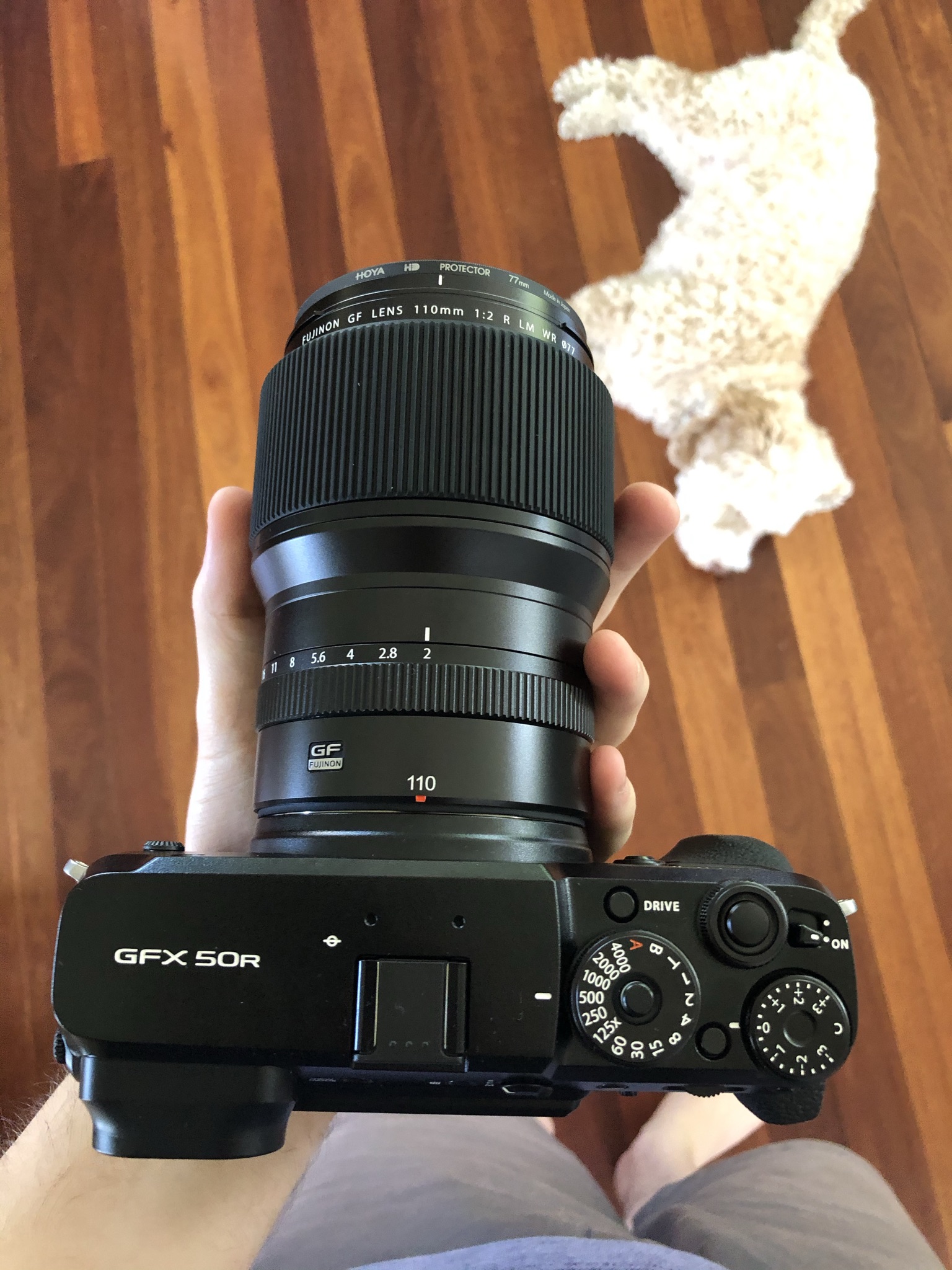
The Fujifilm GFX line of cameras is the most accessible digital 'medium format' system to date, and the Fujinon lenses are optically fantastic and incredibly capable.
While there are a handful of dumb mechanical lens adaptors for the G-mount, and a couple of 'smart' adaptors from companies like Fringer, there is very little information about the mount or protocol.
I had a 'the right kind of wrong' idea to figure out GF lens control with the end-goal of (possibly) building a 'medium format' film camera around them.
As all of the currently released GF lenses use fly-by-wire focus, electronic aperture, and some need to be powered up to position floating optical elements - if I want to build a camera around them then I'll need to reverse engineer the mechanical, electrical, and software to even consider camera design.
Disassembling a MCEX-45G
I picked up the 45mm extension tube on a ~25% discount with the intention of using it to bootstrap debugging, and probably provide donor lens/body mount flanges.
Can confirm it works as advertised with the GF 110mm F2.

Lets dive in.
Lens mount basics
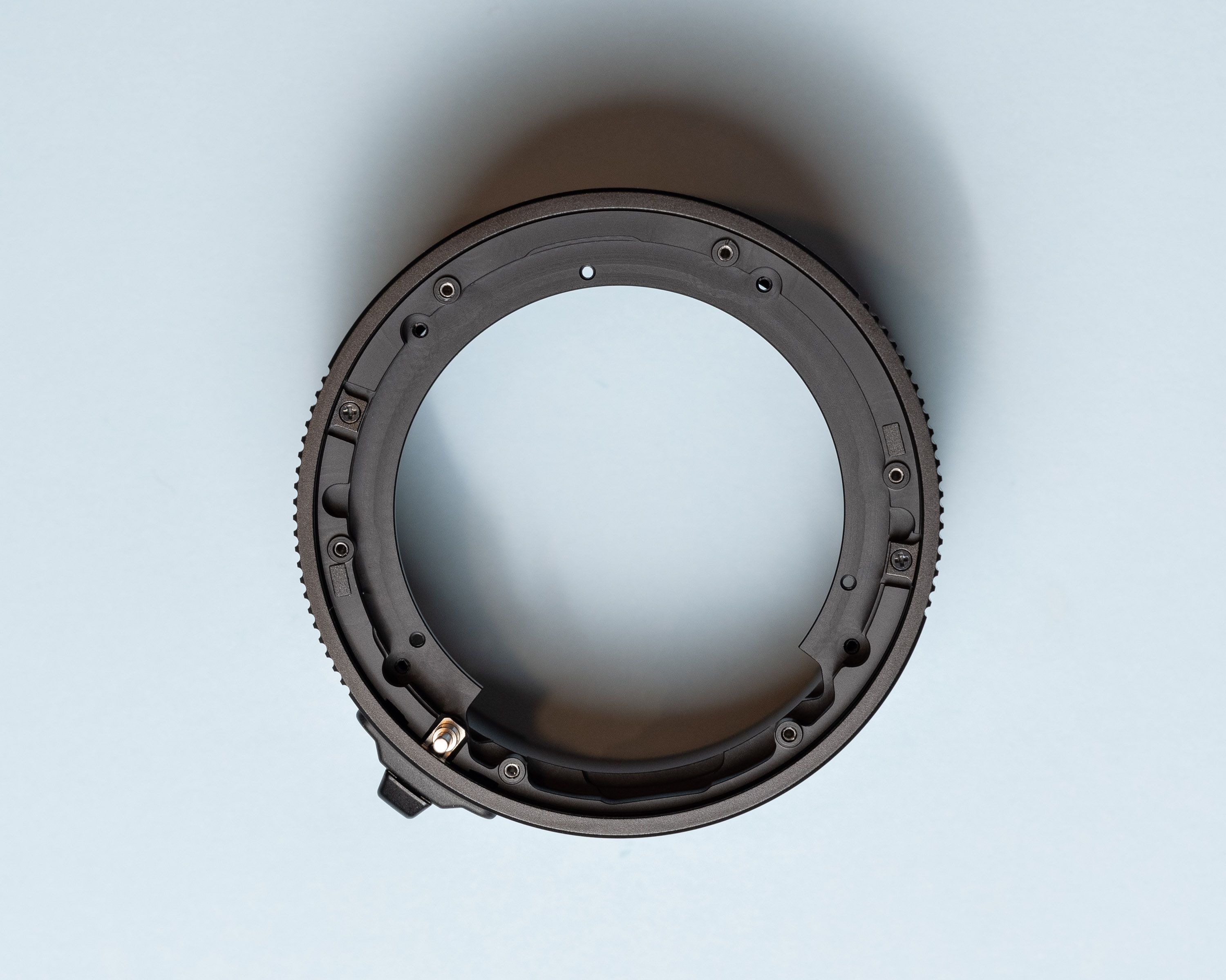
The electrical connections between the body and lens are made with 12 spring loaded contacts on the body which mechanically align with 11 contact rectangles on the lens.
My reference drawing for the lens contacts:
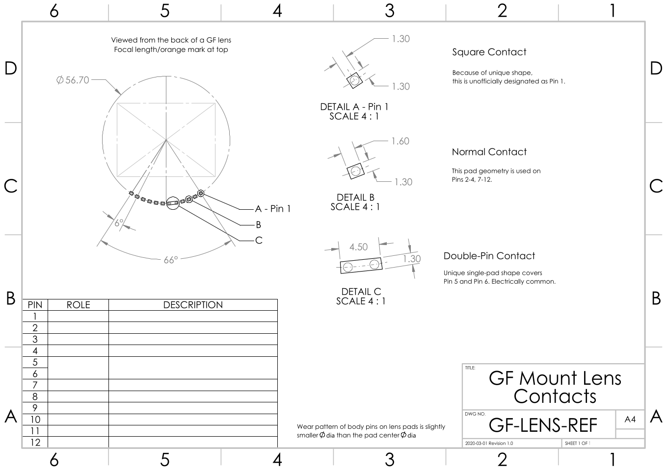
Lens Side
The lens-side contacts are 1.6 x 1.3 mm rectangular pads, with the long edge aligned tangentially to the circular mount.
When looking at the back of the lens mount, the right-most pin is a 1.3 mm x 1.3 mm square contact.
- For ease of convention, I'll label this square pad as
Pin 1, though I don't know what the official nomenclature is.
- For ease of convention, I'll label this square pad as
Based on this numbering scheme,
Pin 5andPin 6are mechanically the same contact rectangle, and therefore electrically common.- Unlike the body side mount, the lens mount/bayonet is not electrically common with
Pin 5andPin 6.
- Unlike the body side mount, the lens mount/bayonet is not electrically common with
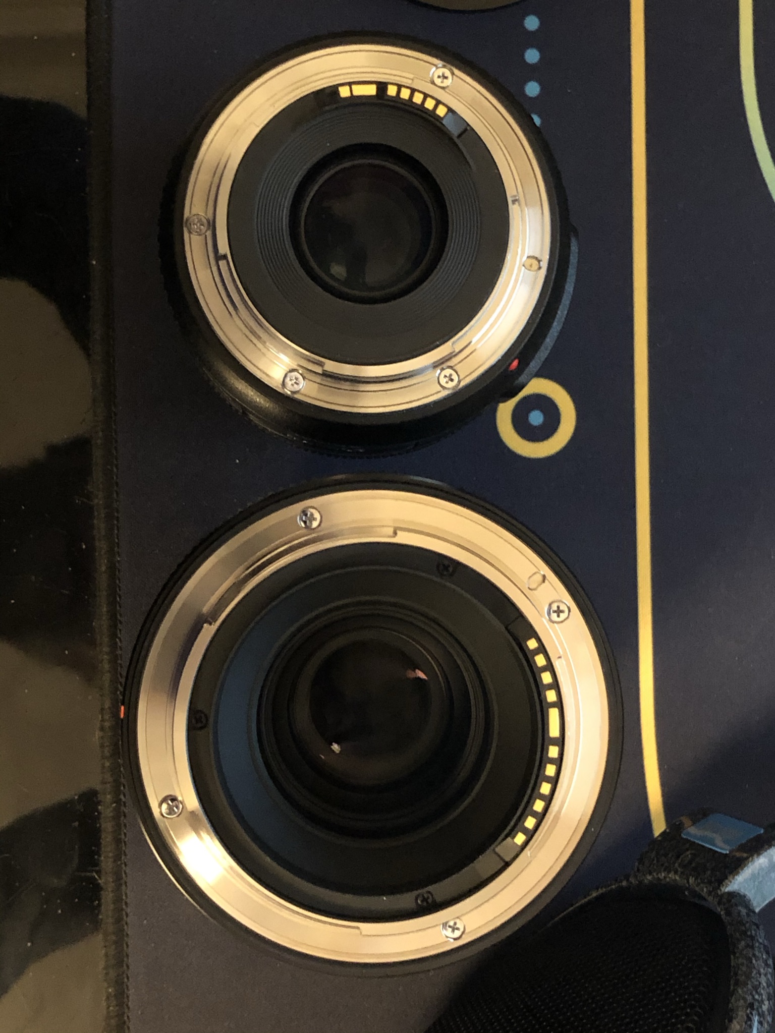
One interesting point to note - the pinout for the GF 45mm (top) doesn't use all 12 contacts that the body provides, while the GF 110mm (bottom) does.
Body Side
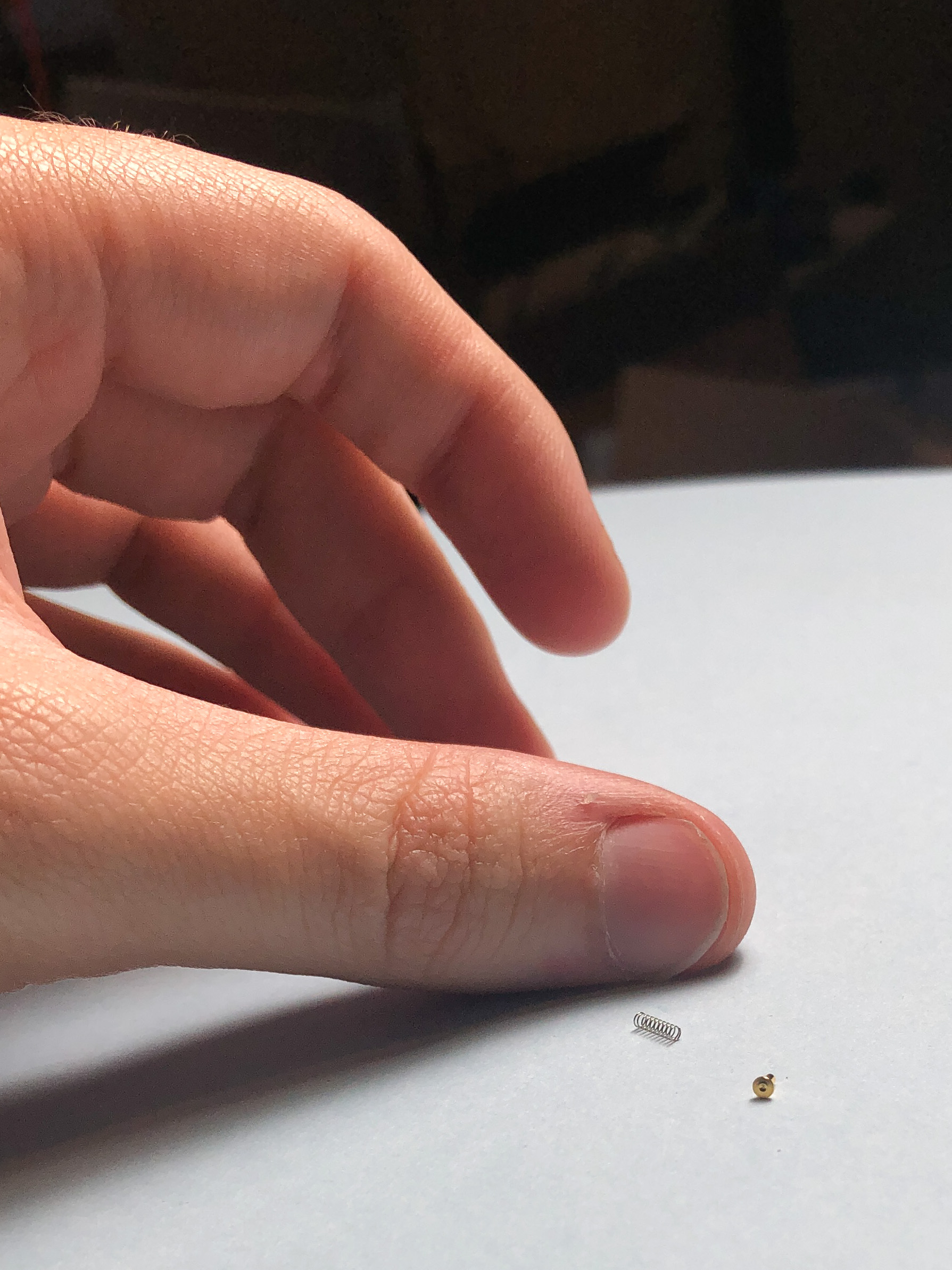
- The spring section of the pins have a 1.0 mm diameter, and a maximum achievable travel of 0.8 mm.
- The spring pins have a conical/round tip.
- The pins are spaced 6° apart, for a total span/range of 66°. There is no pin on the vertical axis, and from a vertical datum aligned with the center of the lens, the outermost edge pins are aligned to +33° and -33°.
- The mount (metal ring/bayonet assembly) is electrically common with the exposed metal inside the battery compartment, as well as
Pin 5andPin 6.
Now lets start opening up the extension tube to learn more...
Tube design
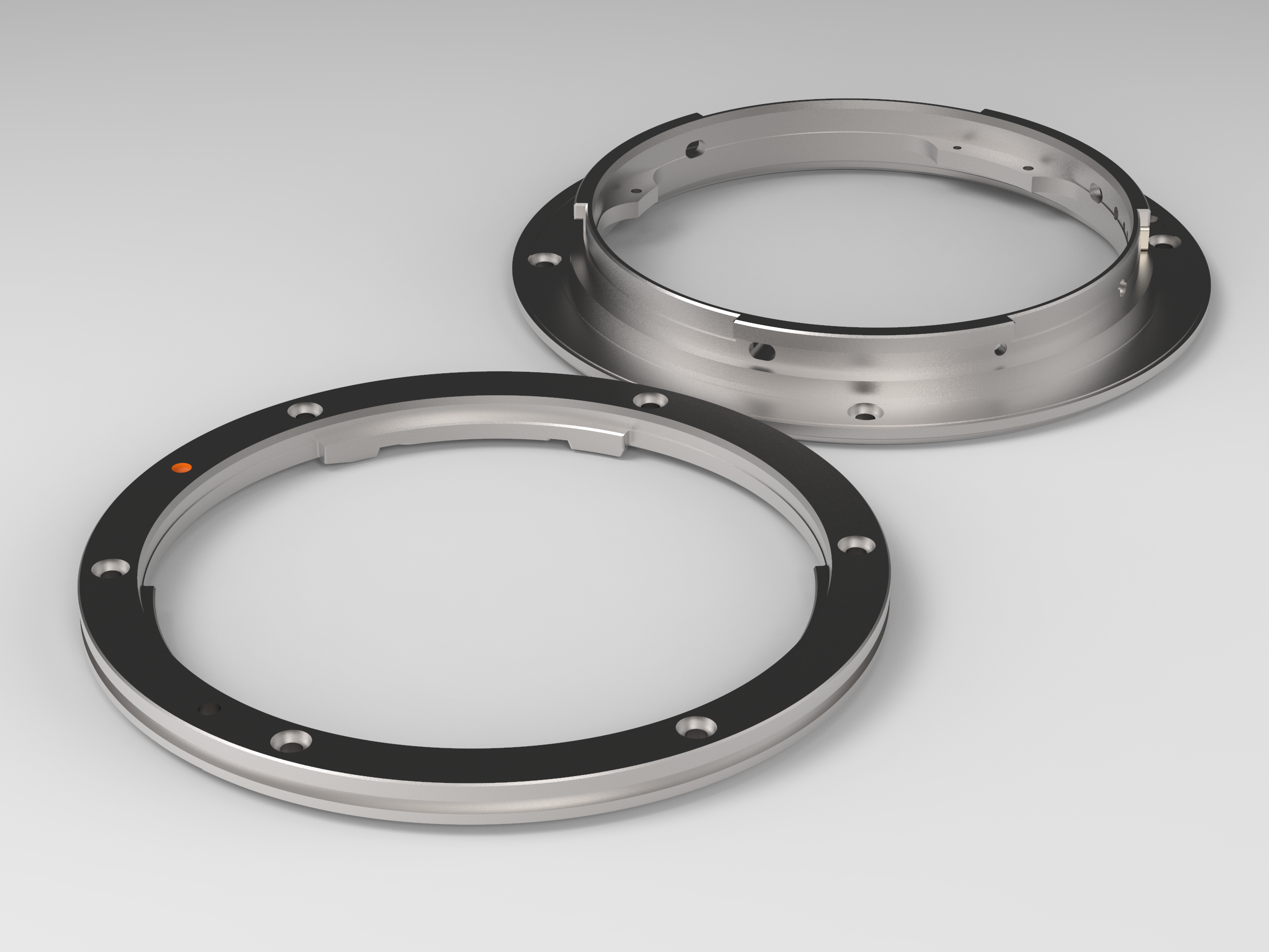
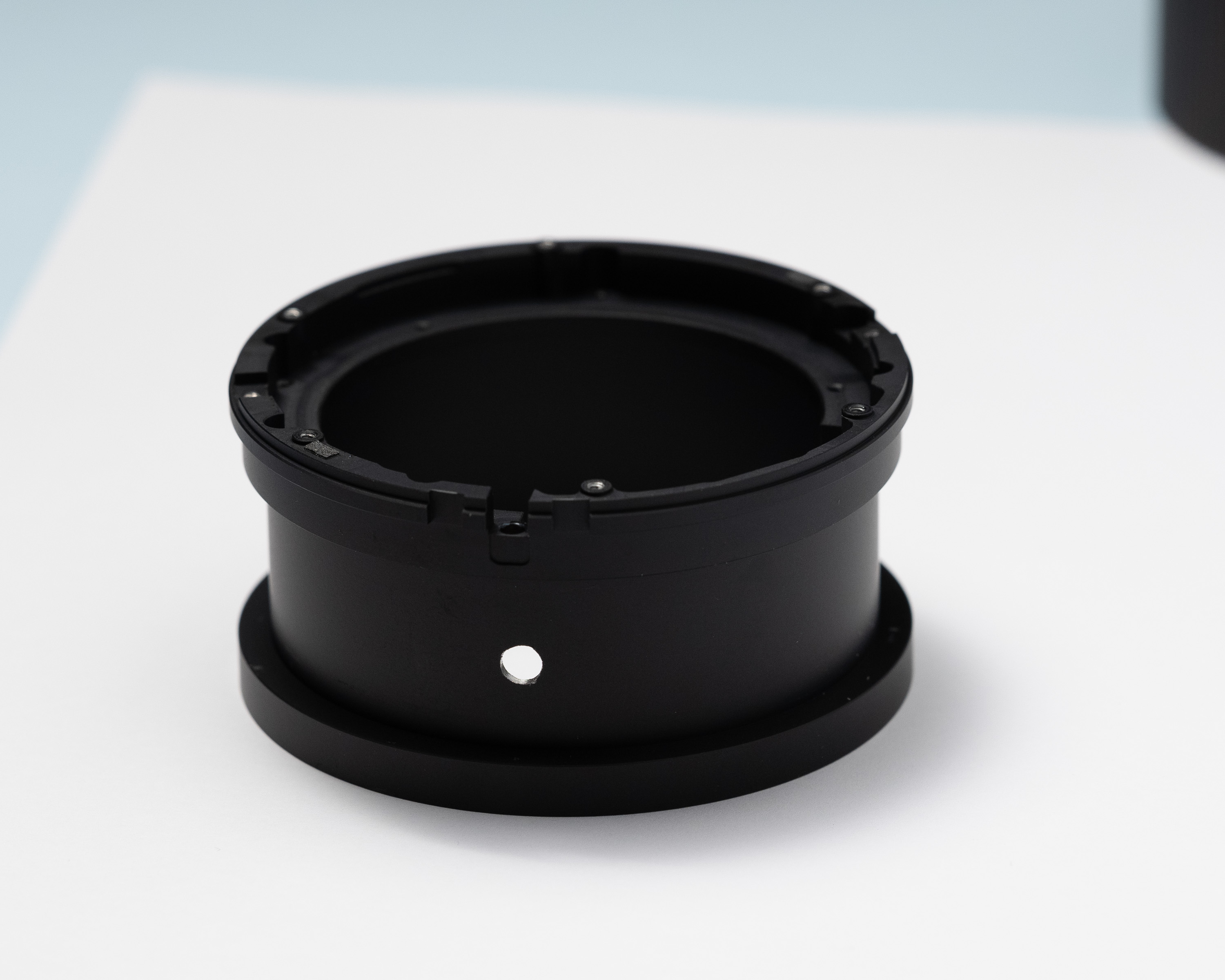
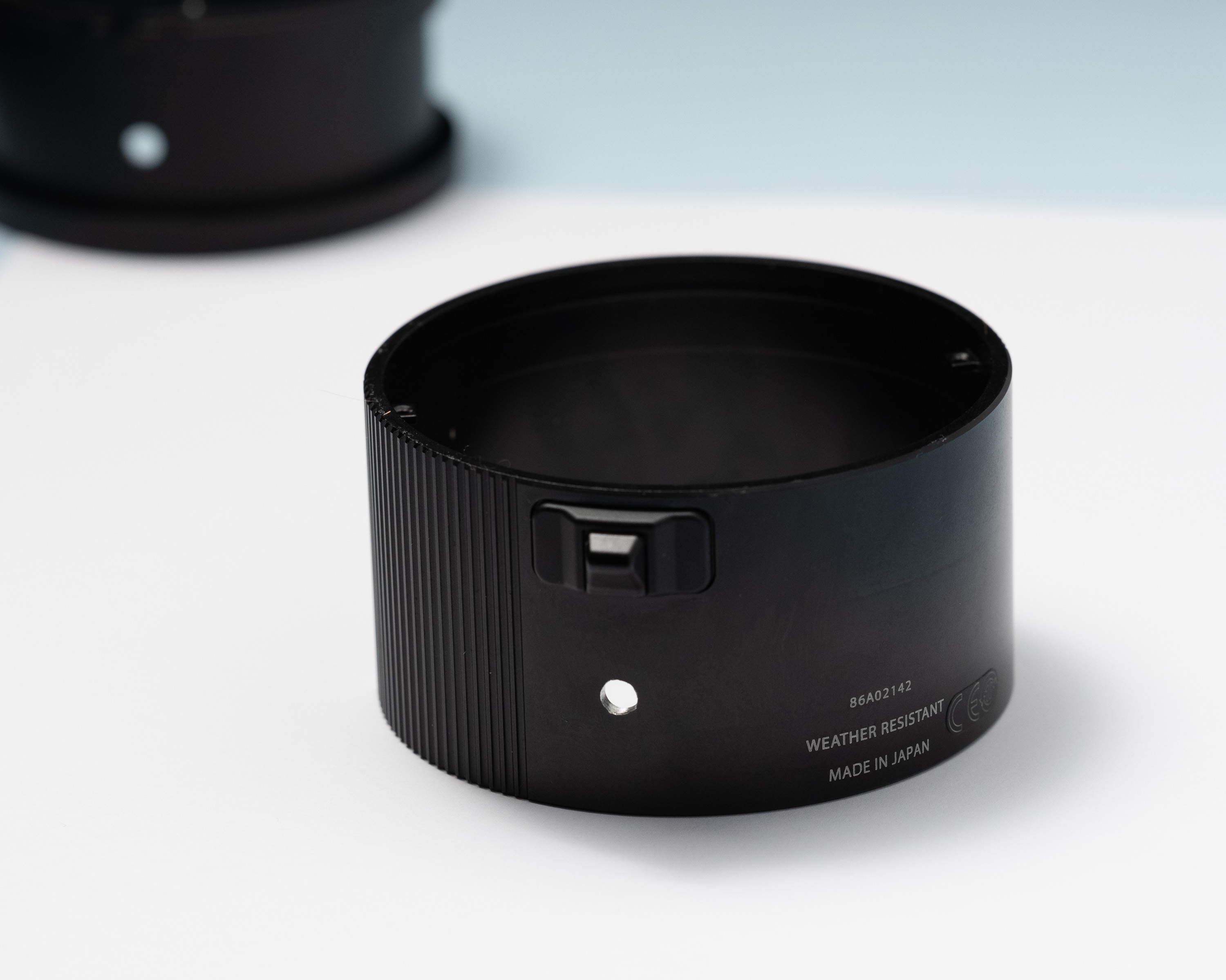
From the rear, a few screws remove the bayonet mount (i.e. the 'lens side mount'). The weathersealing gasket slides off with it, and we can see the simple internal design of the extension tube.
Looking into the cavity, there are some small screws which allow the removal of the internal baffle cylinder piece.
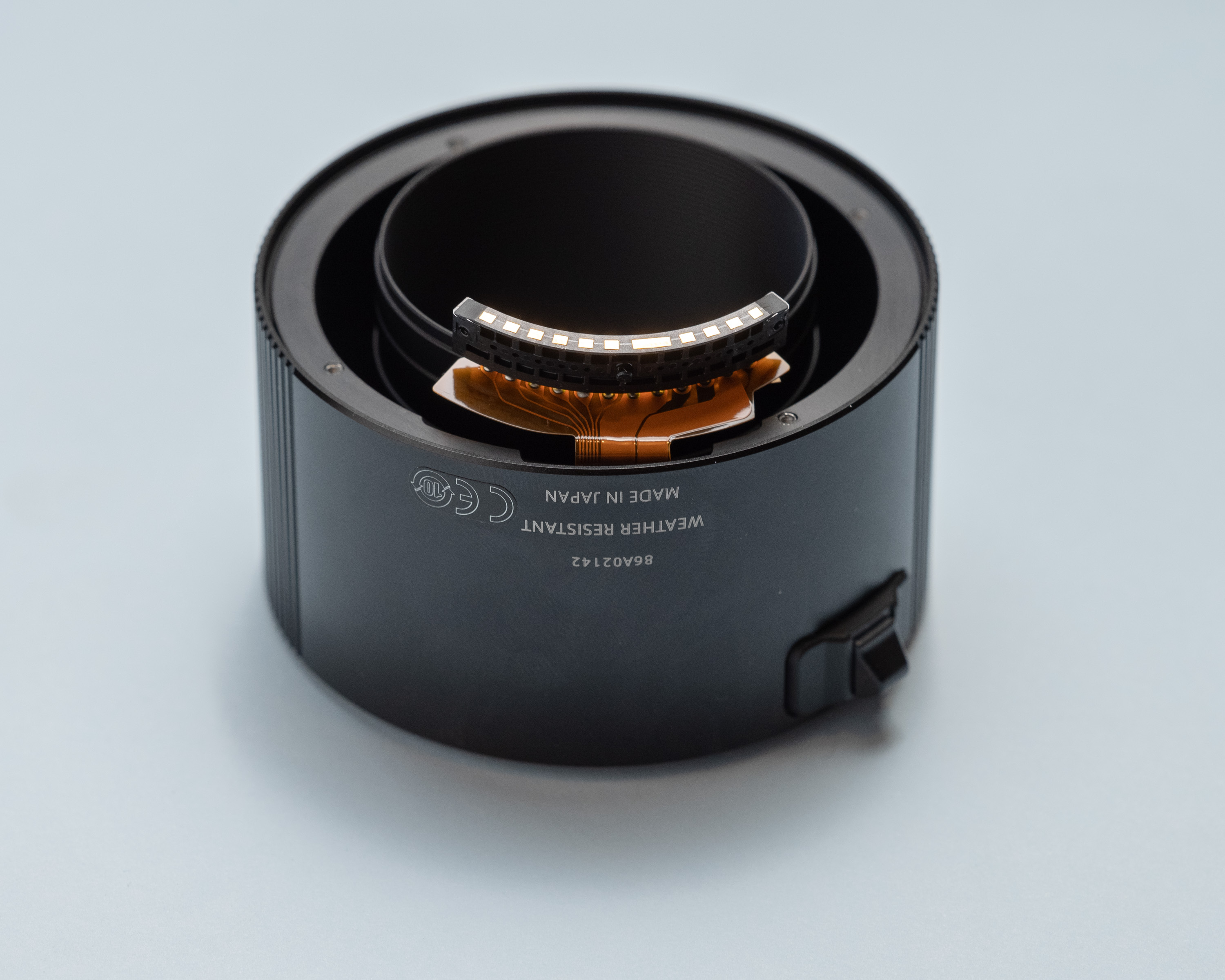
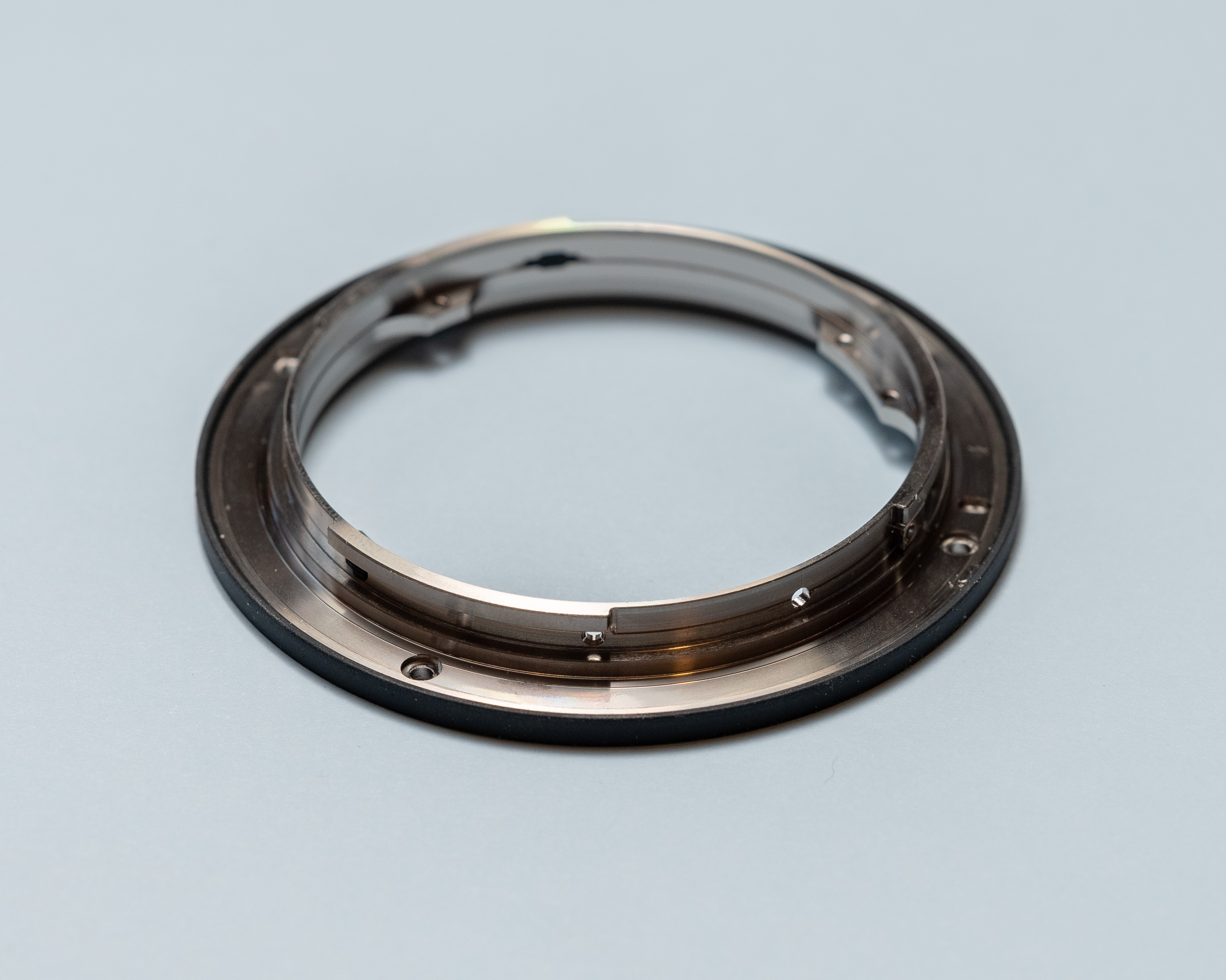
The 'female' flange assembly which is found on the camera body has a machined mating face and orange lens alignment dot, backed by a thin spring plate to provide preload against the incoming lens bayonet features.
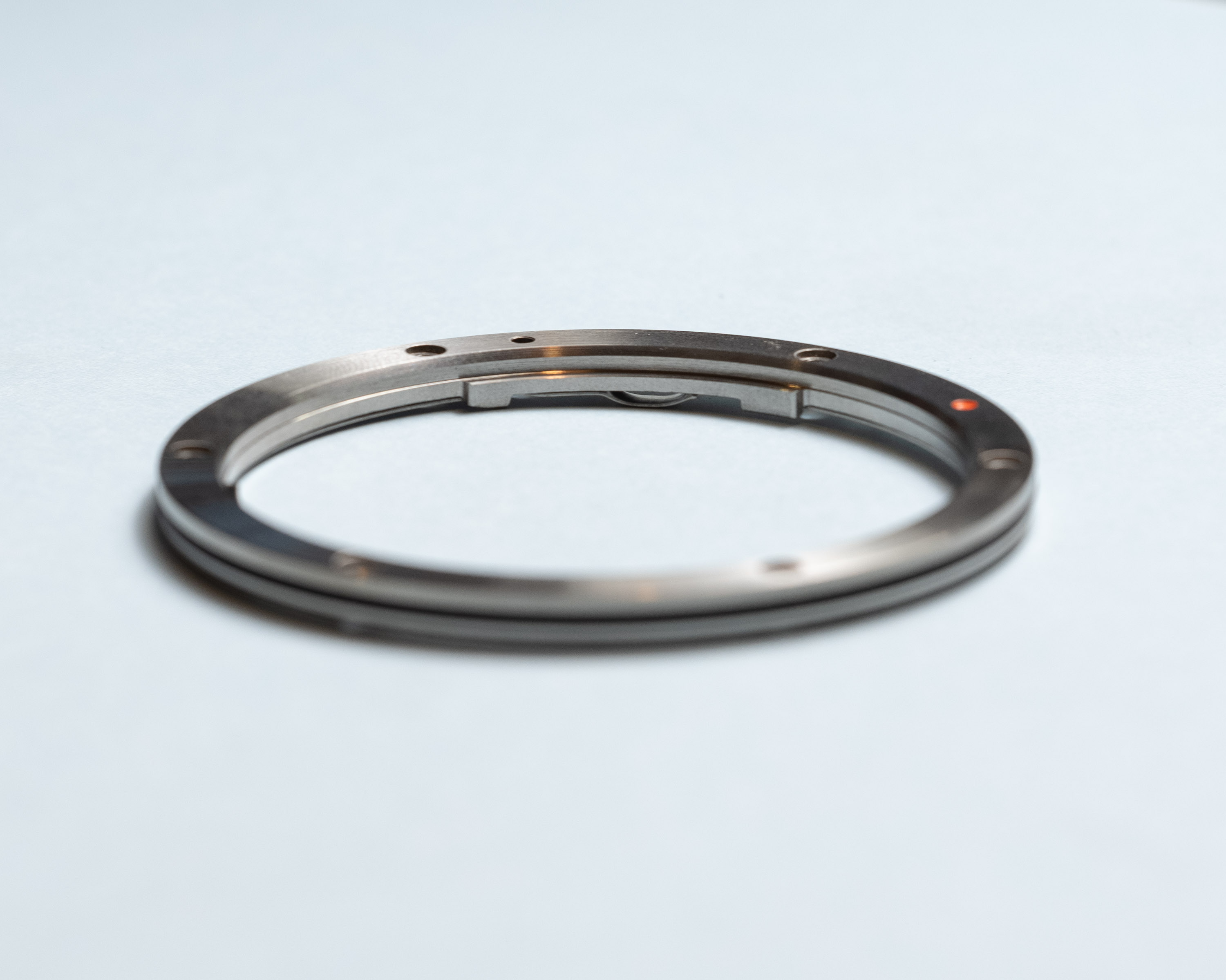
The lens release is a simple spring loaded post that just rests against the main tube assembly.
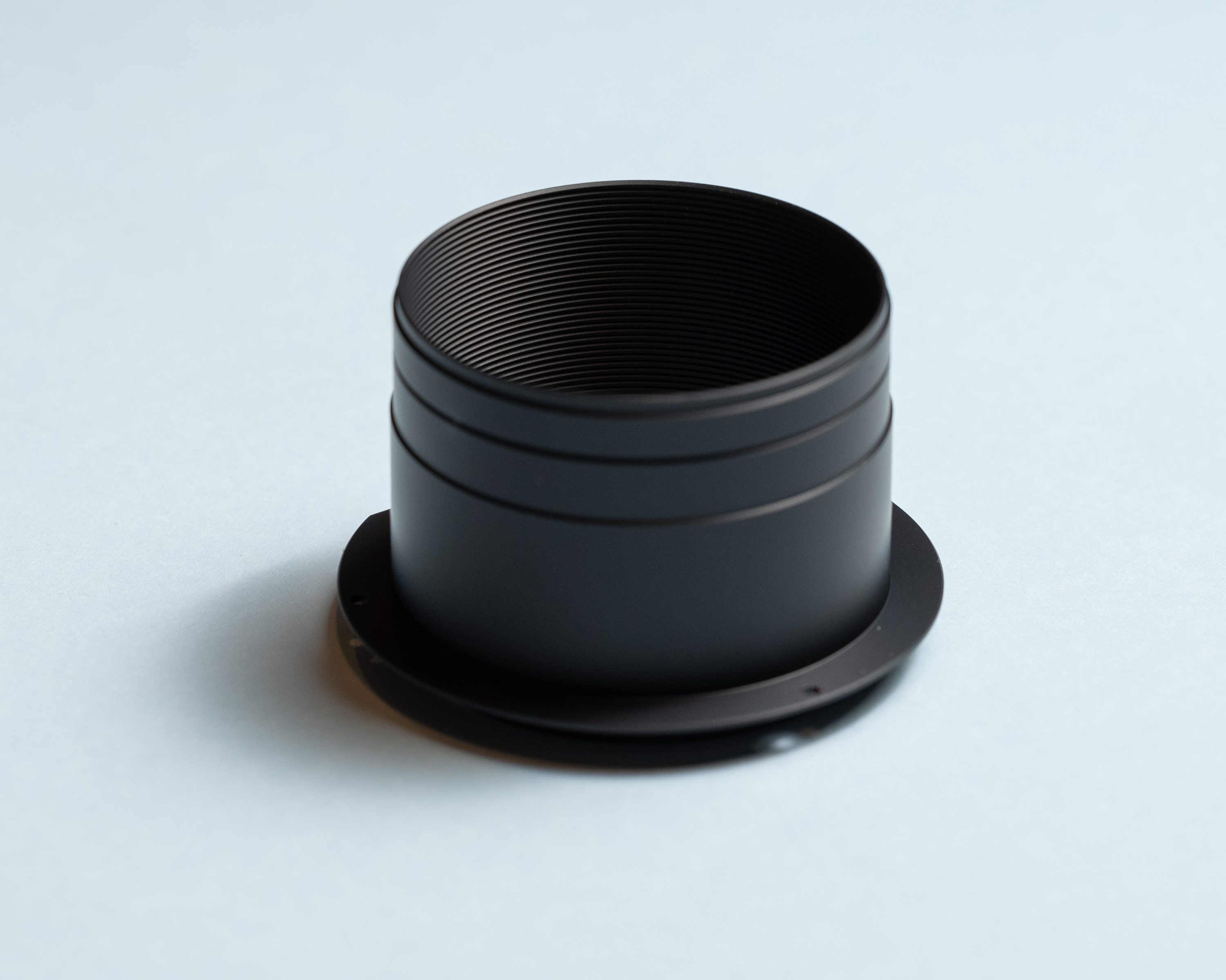
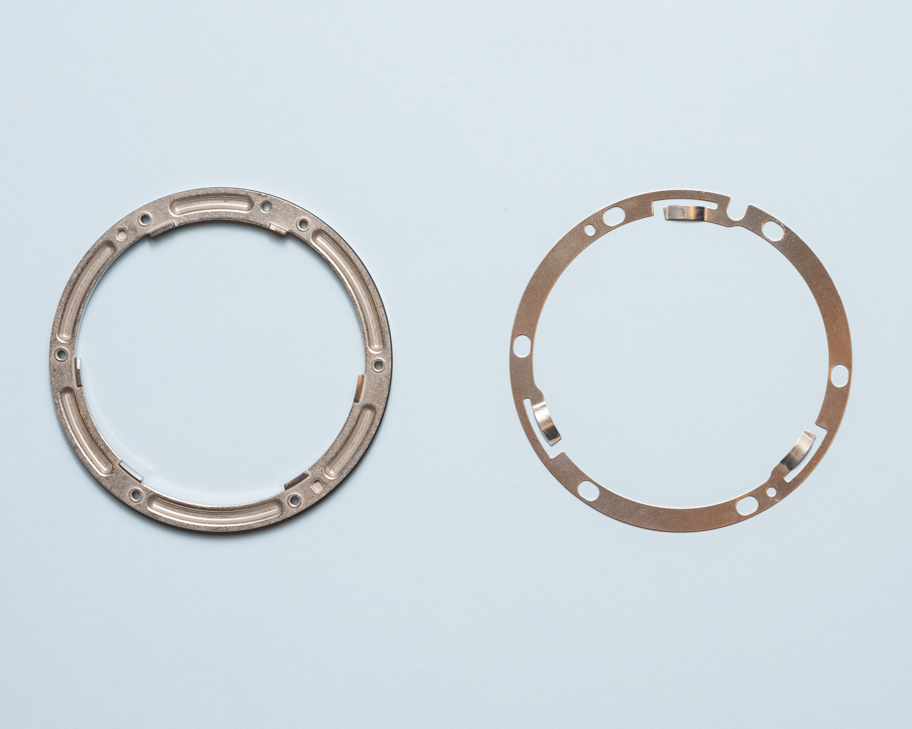
The main tube assembly is actually two pieces - the thin exterior 'skin', and a thicker machined aluminium piece which has most of the mounting geometry for the mounting flanges and electrical sub-assembly.
CAD Models
I took a handful of measurements of each mount and attempted to draw mechanically compatible lens and body mount designs in Solidworks.
I'm not 100% on the accuracy of either design, but a motion study showed them mating successfully and I'm confident I'd be able to use these as a starting point for a more manufacture-friendly design.
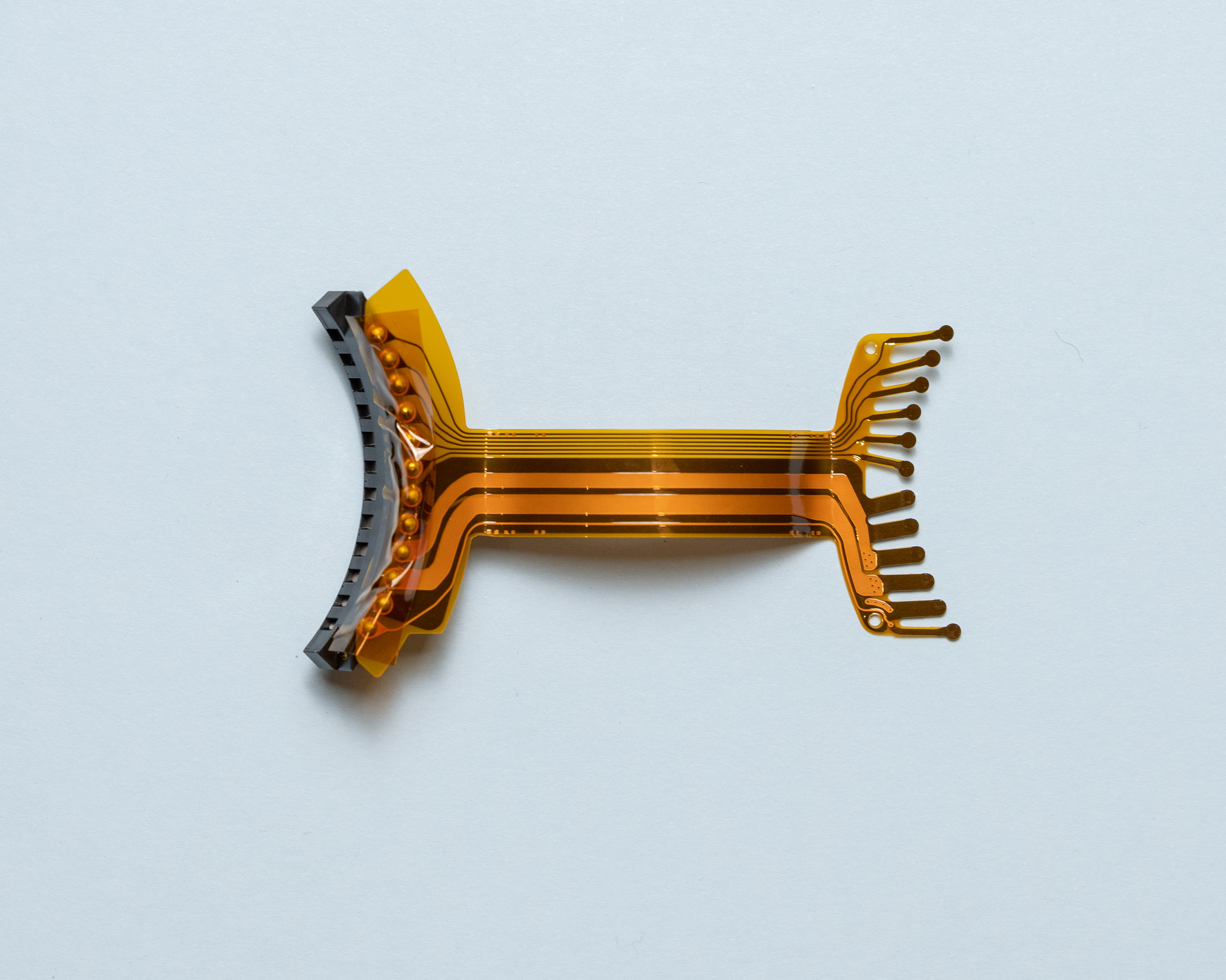
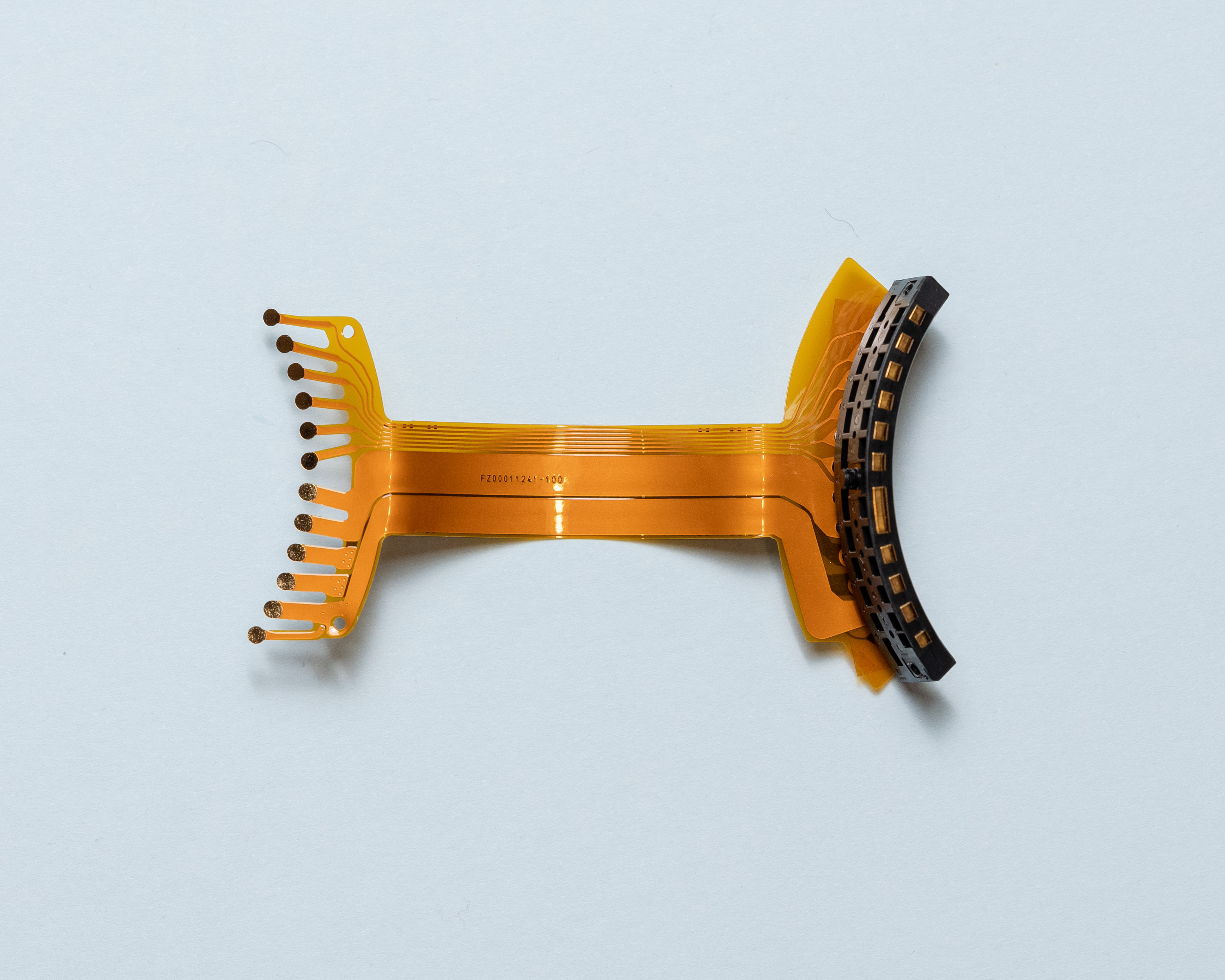
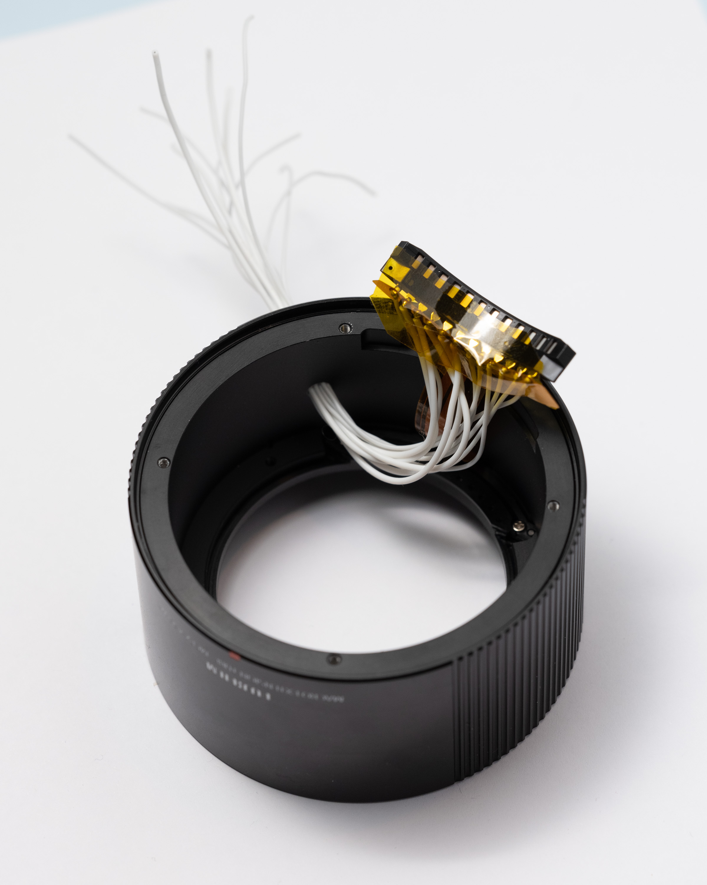
Flex PCB
As we expected before the tear-down, the extension tube only provides a dumb pass-through to the lens mount, there's no active electronics.
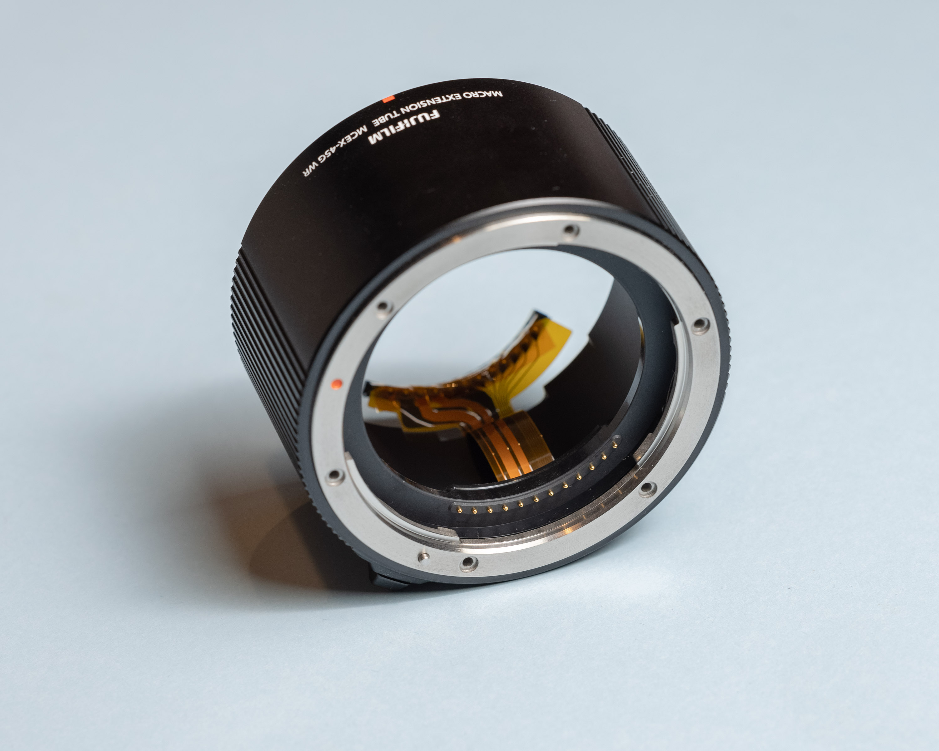
The pad sections of the flex are held captive against a plastic ring which supports some tiny pogo-pins.
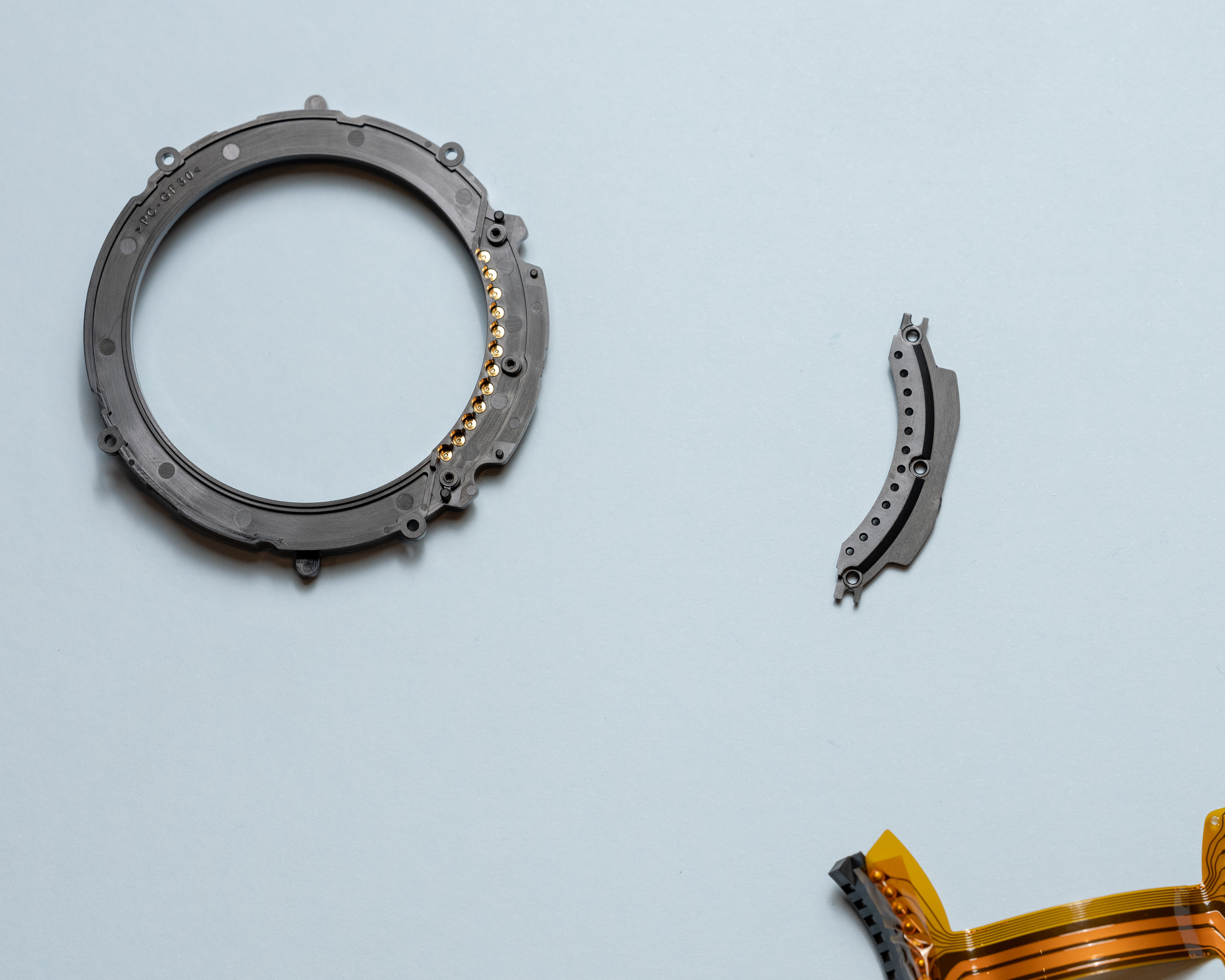
Hindsight tells us that unscrewing the plastic retention bracket behind the pogo-pins is a mistake - I spent the better part of an hour trying to guide the springs back into place with a handmade jig of needles.
We now have some good hints of which pins are responsible for power, and those which are intended for data.
Attaching debug probes
With the electrical sub-assemblies out of the tube we begin by removing the Kapton tape protecting the through-hole pins, solder silicone wires onto the camera side of the flex, and then re-apply fresh Kapton tape to protect the joins from electrical contact with the tube/mount.
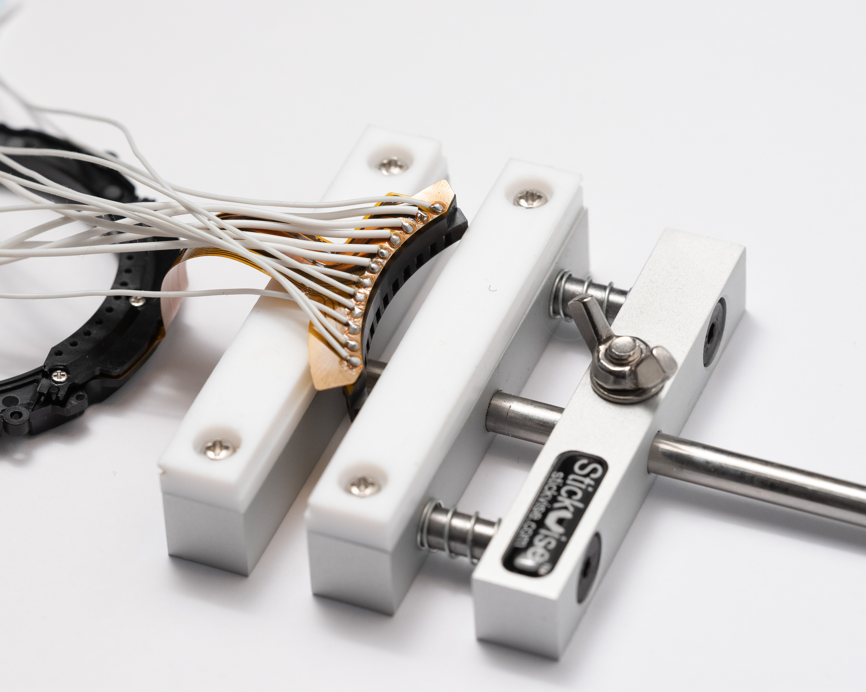
But you might be asking, "how do you get the wires out of a sealed tube"?
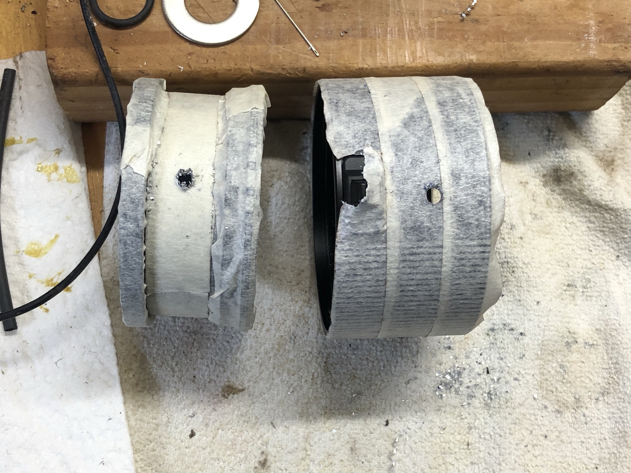
With the exit holes measured and drilled, I started re-assembling the extension tube.
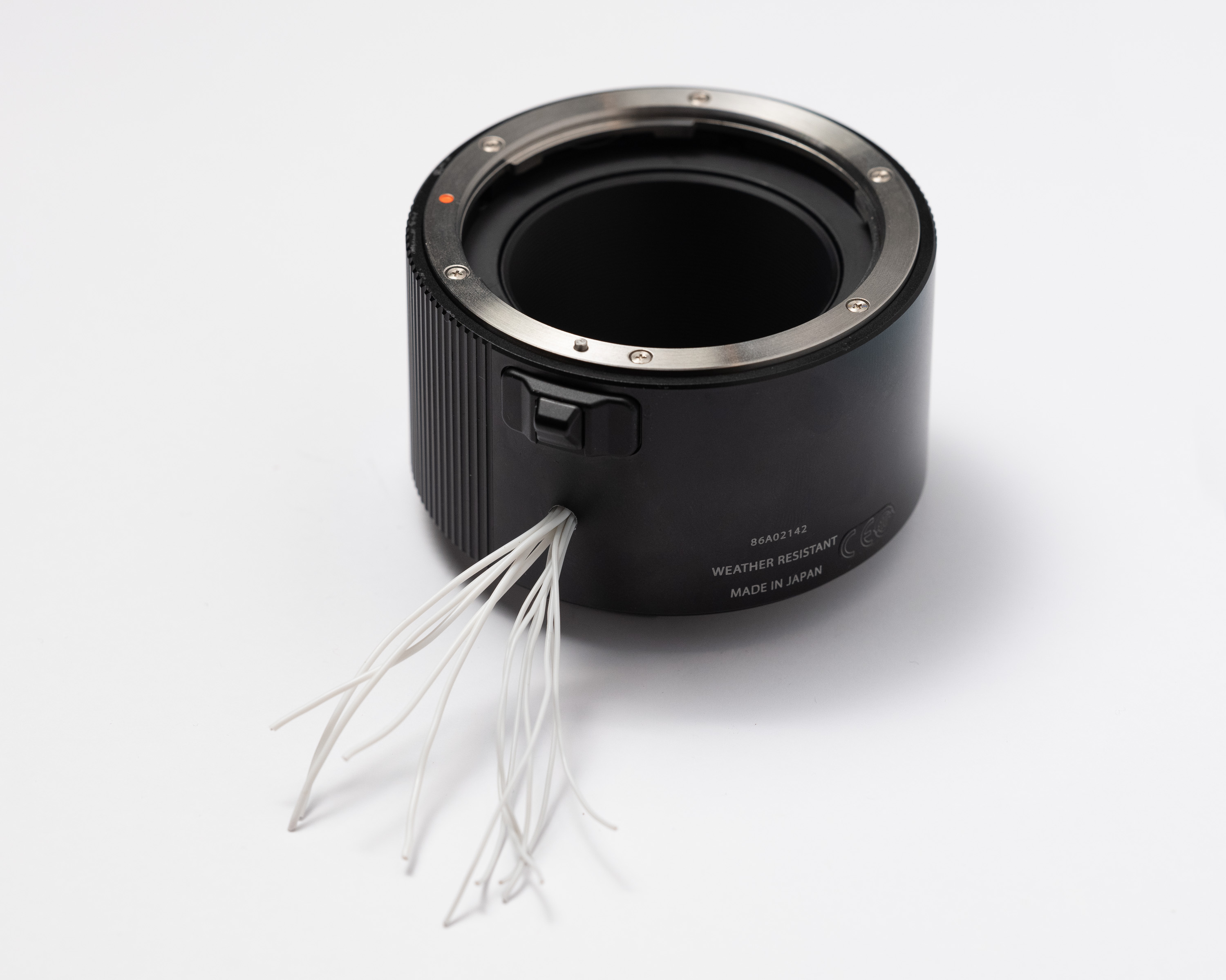
Once the tube was re-assembled, I identified each debug wire by checking for continuity with the lens mount pins, and then soldered on a terminal strip to make debug connections easier.
Electrical Behaviour
We'll start by identifying our power pins. Some immediate clues can be gleaned from looking at the flex PCB and by probing the pins on the camera.
The ground was assumed to be Pin 5 as it has higher-current traces and is common with Pin 6 on the lens mount side. It's also electrically common with the GFX body mount. A quick poke around with a multimeter and oscilloscope for a few minutes shows the ~8V battery voltage on Pin 4, with 5.3V on Pin2 and 6.7V on Pin 3.
The thinner signal lines seem to be 3.3V logic level, so I now know it's safe to connect to the logic analyser and can start sniffing for communications between the body and lens.
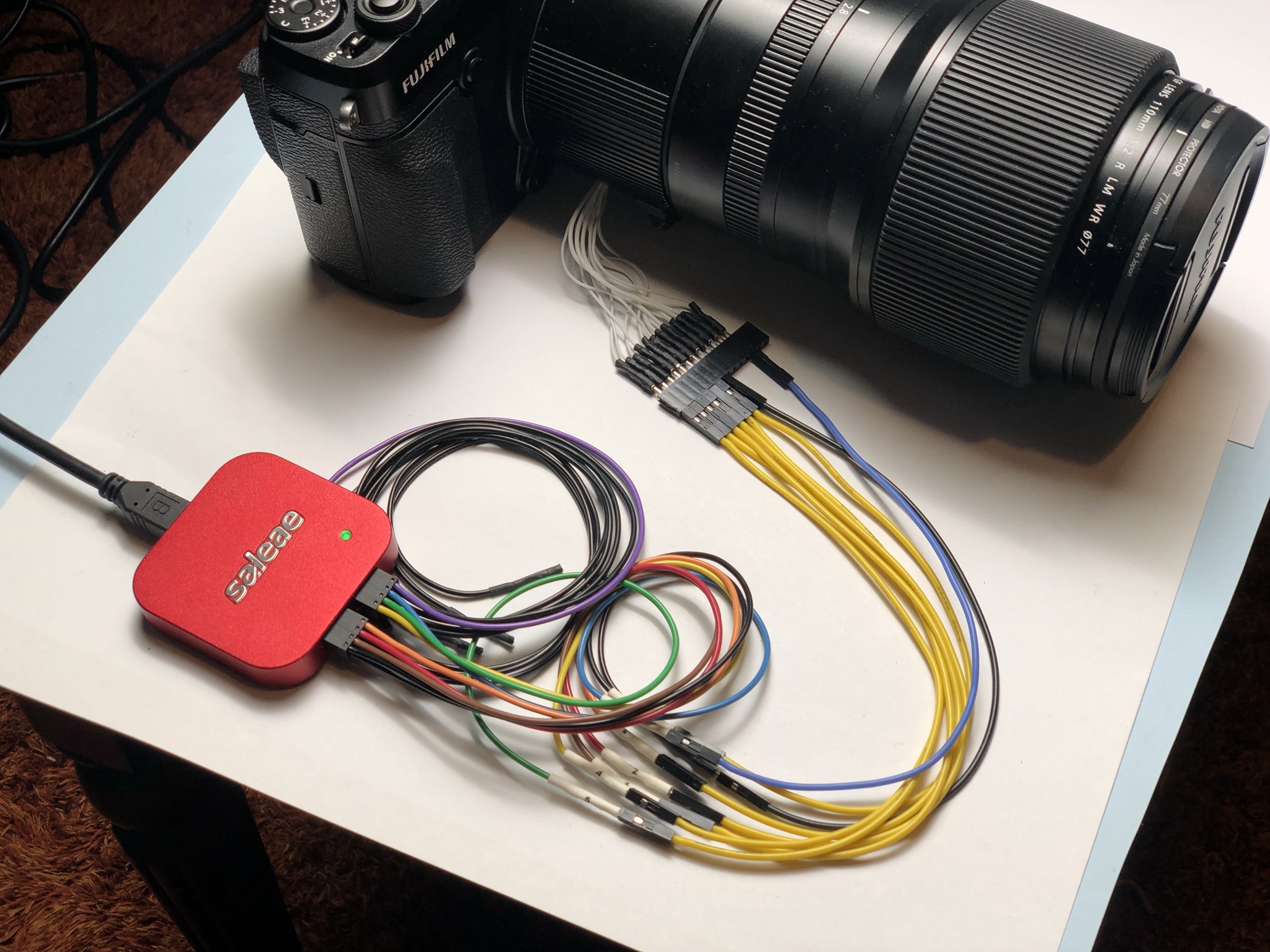
I captured a simple camera operation to start off the analysis, power up, focus, take a photo, and then power-off as this should cover a most 'common' behaviours.
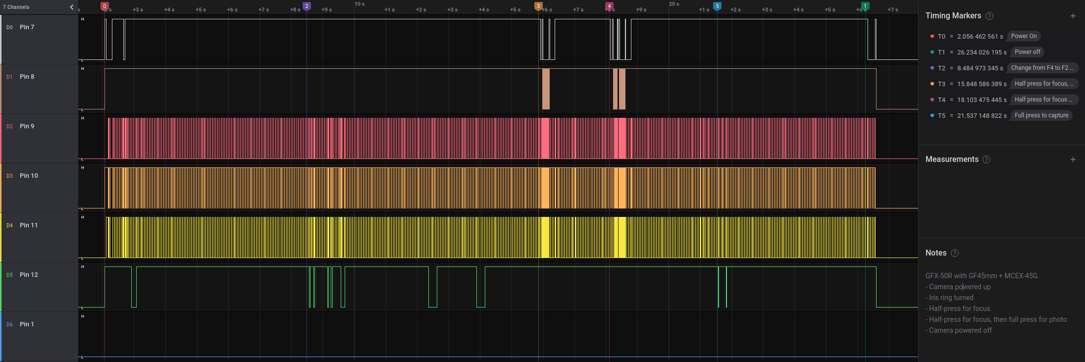
Lets start by looking into the data lines first. We can see some one-way data transfers, as well as request/response style behaviour. This lets us make the following observations about these data pins:
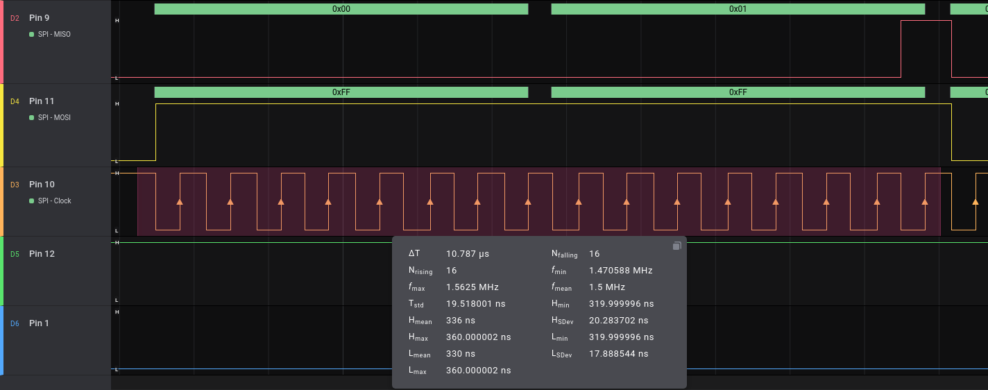
Pin 9is the body's DATA OUT line,Pin 10is a 1.5MHz SPI-style clock signal,Pin 11is the body's DATA IN line,
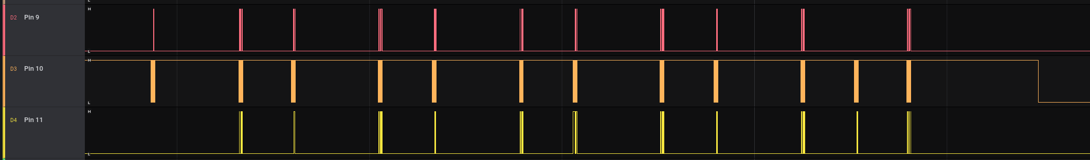
With this in mind, lets identify the properties of the communications bus and determine if it's a fairly typical SPI or some Fuji special sauce:
- A transaction seems to consist of 32-bits at minimum,
- Almost all transactions are 32-bits long.
- During startup, a pair of 1048-bit long transactions occur with a 3ms gap - these are the longest identified transactions.
- As the division of
1048and the potential bits-per-transfer should be an integer, we can reasonably throw out16and32bit transfer sizes. - Therefore it's reasonable to assume byte-level layout of packets.
- We can also determine the clock behaviour, by looking at the first falling edge and any 8-bit aligned end:
- The clock is high when inactive (CPOL = 1).
- Data appears to be timed for the clock's trailing edge (CPHA = 1)
The other IO lines are less immediately obvious,
Pin 1is intended as a signalling line due to the trace thickness, but I saw no activity.- Could be a signal GND line? Or I need some other lens to find a use for it?
Pin 7seems to be related to auto-focus motor activation.Pin 12correlates to the iris closing.
So my unofficial pinout is:
| Pin | Voltage | State | Scope/Notes |
|---|---|---|---|
| 1 | ~0V | Never triggers scope, even with varied stimulus/settings. | |
| 2 | 5.32V | DC | |
| 3 | 6.72V | DC | |
| 4 | 8.01V | DC | Battery Voltage. ~100mV ripple when focus motor engages. |
| 5 | - | - | GND |
| 6 | - | - | Electrically common with Pin 5 |
| 7 | 3.4V | Normally high | Infrequent squarewave. No recognisable pattern. |
| 8 | 3.38V | Normally high | High speed edges, infrequently triggered. Pulses LOW for approx 100-350ns at a 10ms interval. |
| 9 | 0V | Normally low | Body DATA OUT. |
| 10 | 3.3V | Normally high | 1.5MHz clock signal |
| 11 | 0V | Normally low | Body DATA IN |
| 12 | 3.3V | Normally high | Squarewave, goes low when iris closes. |
Protocol Analysis
We can now sniff the packets being sent between the lens and body. I took quite a while to build a library of captures for both of my lenses with the minimal amount of state change in each to make isolating unique packets easier:
- Spinning the focus ring in auto-focus mode and manual mode
- Changing the aperture selection ring with and without depth-of-field preview active
- Changing the auto-focus mode switch between single/continuous/manual
- Entering and exiting playback mode, sleep mode, OVF active
- Sweeps of focus position in manual and AF modes
- AF refocus behaviours at different depths and light levels to make it hunt
From a few test captures, almost all packets are 4-bytes long with the last byte looking rather unstable so I'm treating it as a checksum. During startup there's a few longer packet sequences that are immediately obvious starting points.
Startup/Identification packets
After the camera is powered on with a GF 45mm F2.8 lens, a series of 131B transactions occur (each sent twice 3ms apart). These transactions are from the lens to the body and describe the lens.
The first transaction starts with 0x00 0x00, the second transaction starts with 0xFF 0xFF. Both end with what I'm assuming is a single checksum byte.
The payload (hex formatted) looks like this:
00000000: 00 00 4c 52 31 30 36 41 00 00 46 53 53 4e 57 30  ..LR106A..FSSNW0
00000010: 30 36 47 46 34 35 6d 6d 46 32 2e 38 20 52 20 57  06GF45mmF2.8 R W
00000020: 52 00 00 00 00 00 00 00 00 00 00 00 00 00 00 00  R...............
00000030: 00 00 00 00 00 00 00 00 00 00 00 00 00 00 00 00  ................
00000040: 00 00 00 00 00 00 00 00 00 00 00 00 00 00 00 00  ................
00000050: 00 00 32 34 30 33 33 38 36 36 30 35 01 56 01 00  ..2403386605.V..
00000060: 01 00 01 00 01 00 c8 01 00 00 00 00 00 00 00 00  ................
00000070: 00 00 00 00 00 00 00 00 00 00 00 00 00 00 00 00  ................
00000080: 00 00 af ...- The first chunk of data is ASCII:
- Not sure what the first string section
LR106A FSSNW006means yet. - Part of the last section is obvious as the lens is officially labelled as
GF45mmF2.8 R WR.
- Not sure what the first string section
- The second block of data in the payload is likely some combination of binary data and potentially ASCII formatted numbers with no obvious meaning.
Sniffing the GF 110mm F2 startup packet we see similar behaviour:
00000000: 00 00 4c 52 31 30 34 41 00 00 46 53 53 4e 57 31  ..LR104A..FSSNW1
00000010: 30 34 47 46 31 31 30 6d 6d 46 32 20 52 20 4c 4d  04GF110mmF2 R LM
00000020: 20 57 52 00 00 00 00 00 00 00 00 00 00 00 00 00   WR.............
00000030: 00 00 00 00 00 00 00 00 00 00 00 00 00 00 00 00  ................
00000040: 00 00 00 00 00 00 00 00 00 00 00 00 00 00 00 00  ................
00000050: 00 00 30 35 43 30 30 30 32 34 00 00 01 60 01 10  ..05C00024...`..
00000060: 01 10 01 10 01 10 c8 01 00 00 00 00 00 00 00 00  ................
00000070: 00 00 00 00 00 00 00 00 00 00 00 00 00 00 00 00  ................
00000080: 00 00 0b ...- The first section of data is ASCII:
LR104A FSSNW104GF110mmF2 R LM WR - The second block is different and similarly unrecognisable.
After the lens packets, and only when the GF110mm is mounted, the camera body describes itself to the lens.
00000000: 00 00 53 50 58 33 00 00 00 00 00 00 47 46 58 20  ..SPX3......GFX
00000010: 35 30 52 00 00 00 00 00 00 00 00 00 00 00 00 00  50R.............
00000020: 47 46 58 20 35 30 52 00 00 00 00 00 00 00 00 35  GFX 50R........5
00000030: 39 33 35 33 34 33 38 33 36 33 31 31 38 31 31 31  9353438363118111
00000040: 33 39 37 44 30 31 30 31 31 30 38 34 31 02 20 01  397D010110841. .
00000050: 35 01 00 01 00 01 00 00 00 00 00 00 00 00 00 00  5...............
00000060: 00 00 00 00 00 00 00 00 00 00 00 00 00 00 00 00  ................
00000070: 00 00 00 00 00 00 00 00 00 00 00 00 00 00 00 00  ................
00000080: 00 00 19 ...- The first section of data is ASCII again
- Unsure of what
SPX3represents. - The repeated pair of
GFX 50Rstring sequences match the body under test.
- Unsure of what
- The second chunk of data is another unknown mix of potentially ASCII, and unprintable bytes.
Focus & Iris control rings
With every other captured packet being 4-bytes in length, I needed a way to try narrow down which ones might correlate to actions that I can control like changing one of the control rings, triggering focus or iris actuation.
The easiest batch to explore is the >70 captures with hopefully minimal differences other than the starting and ending aperture selections, along with versions with depth-of-field preview enabled so I could force the lens to actuate when changed. A quick script pulled decoded SPI traffic from the logic analyser captures and sorted for unique 4-byte packets across the different runs.
In the lens-to-body direction, a group of 'seen once' packets basically jumped out, with the second byte value mapping against the control ring's third-stop clicks.
| Control Ring | Index value | Observed packet |
|---|---|---|
| f/2.8 | 0x01 | 00 01 0c 10 |
| f/3.2 | 0x02 | 00 02 0c 32 |
| f/3.6 | 0x03 | 00 03 0c 12 |
| f/8 | 0x0a | 00 0a 0c 3a |
| f/32 | 0x16 | 00 16 0c 06 |
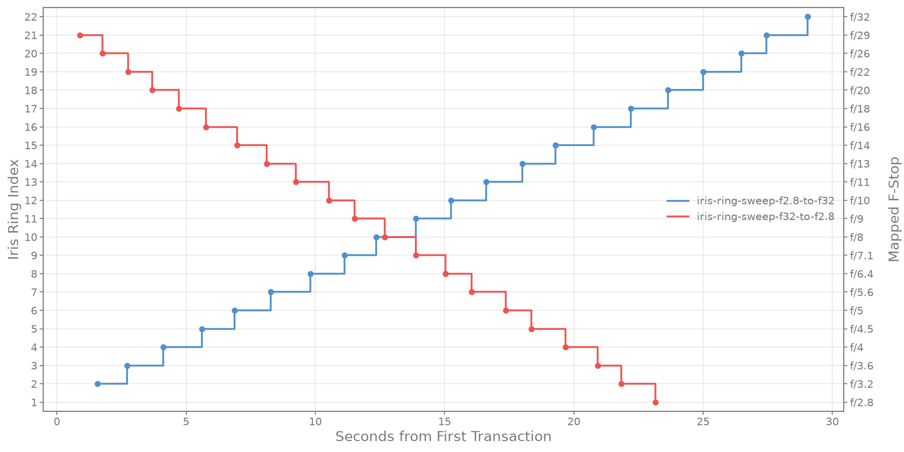
The GF110 F2 maps the same way with f/2.0 at index 1, so the body likely has a way of mapping these indices against f-stop from the version dumps during startup.
While I initially thought 0c might be the 'iris ring' packet identifier, I also found it in focus ring packets. In captures with small, big, fast and repeating moves in both directions those packets seem to encode a big-endian 16-bit value.
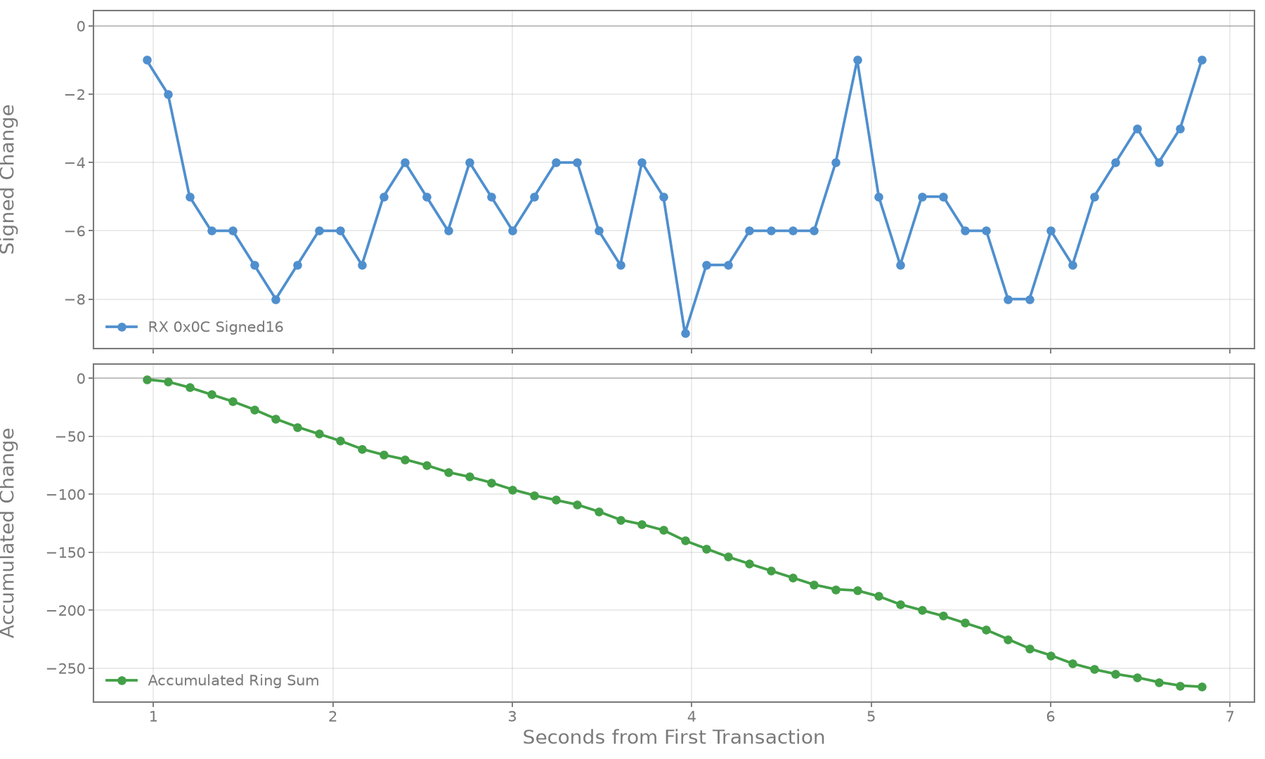
- Clockwise captures are positive values, counterclockwise are negative.
- They are relative values, showing larger values in the 'fast' rotation captures.
- They aren't published or polled at different rates based on magnitude or if a change was reported.
- The behaviour appears the same on the GF45 and GF110mm lenses
00 01 0c 92    +1
00 04 0c b6    +4
00 08 0c ba    +8

ff ff 0c 8c    -1
ff fb 0c 88    -5
ff f8 0c a6    -8
But interestingly, the top-two bits of the last byte have different values for the focus ring than the iris ring captures. So maybe a sub-field to select which control ring? Or a larger address value that's across both bytes?
Focus Motor Packets
I need to understand how the fly-by-wire focus behaviour works if I want to have a chance of doing useful things with these lenses on different bodies. As well as some new packet types, these captures have interrupt like events and a 'motor active' behaviours on two of the digital IO (shaded red on plot).
Looking at a single motor event from the capture, the body sends three control values prior to a synchronisation/actuation command. I'm using the 'tag' wording for the 'upper 2 bits' of the last byte.
tx 03 dc 15 10       Tag 0, unknown value 988 request
rx 00 00 00 00

tx 0f 10 80 1a       ?
rx 08 00 95 28       0x15 family ACK

tx 01 20 15 40       Tag 1, unknown value 288 request
rx 03 dc 15 10       Echo of Slot A request

tx 08 00 95 28       0x15 family ACK
rx 0f 00 95 62       0x15 family ACK

tx 01 ed 15 b2       Tag 2, target position 493
rx 01 20 15 40       Echo of 288 Tag 1

tx 09 00 95 72       0x15 family ACK
rx 08 00 95 aa       0x15 family ACK

tx 00 00 3f c6       Execute/latch
rx 01 ed 15 b2       Echo of target position 493 Tag 2

tx 0a 00 95 ba       ACK/status
rx 09 00 bf e0       Execute ACK

tx 00 00 00 00
rx 00 00 3f c6       Echo of execute
This sequence is very consistent on both the GF45 and GF110 lenses but the values vary. Plotting some of the autofocus captures shows more complex moves with fewer command bursts.
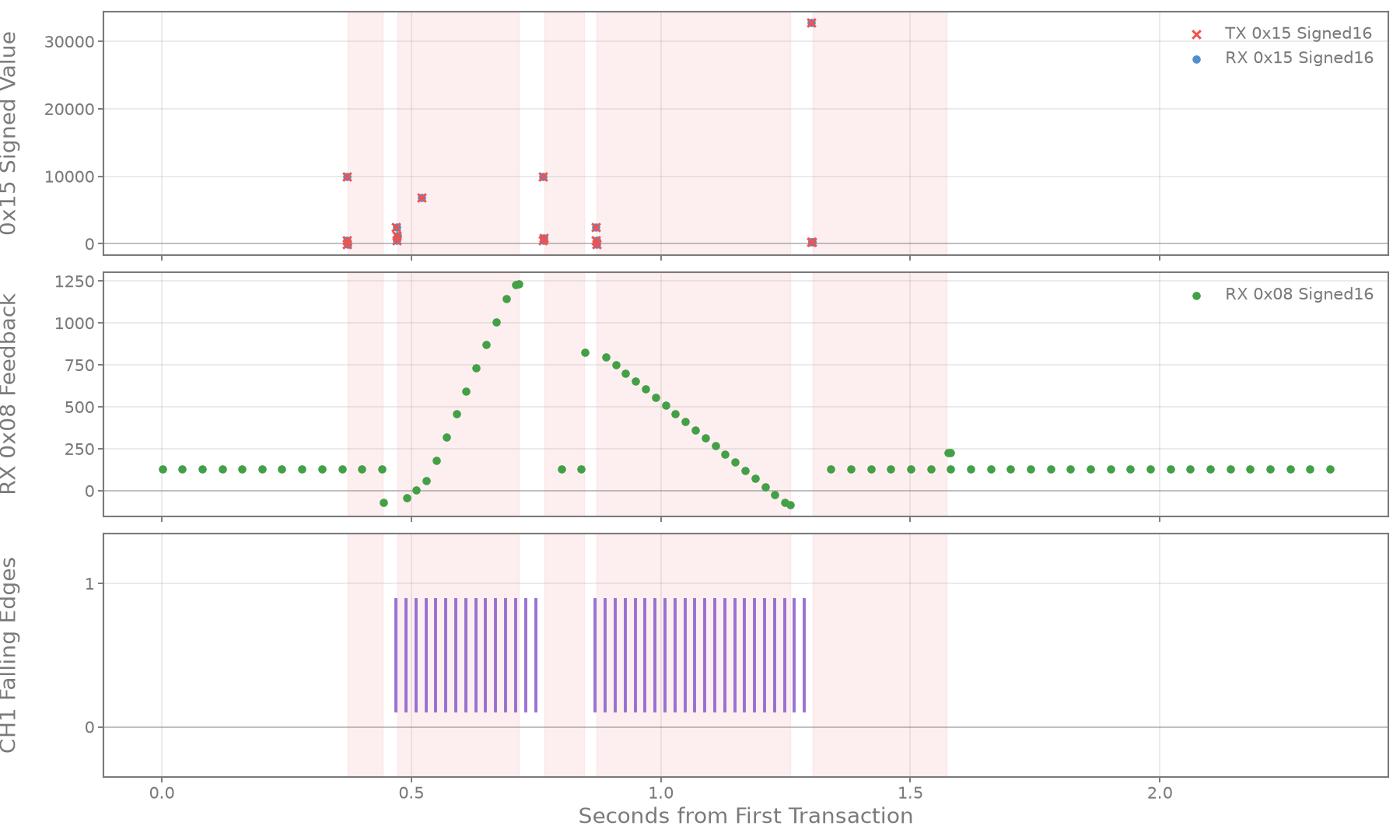
It's a bit hard to work out what the camera is commanding, especially as the position feedback shows different easing curves, but my running theory is the three command values describe:
Envelope, or move budget
- The value doesn't seem to correlate to position,
- Correlates fairly well with the duration of the move, approx ~0.141 ms/count
- Is sometimes a error/infinite value
2^15 - 1 = 32767which is the end of the range7f ff.
Speed/Mode
- It's always
288in manual focus mode, and the motor always makes small quick movements as the ring turns - Autofocus runs on the GF45 and GF110 have the same values
- I don't think my captures were able to cover enough range in focus speed to find correlations though
- It's always
Target position
Like the focus ring, the first two bytes seem to be a signed big-endian 16-bit position value.
Highly correlated to the feedback value (but not identical)
On the 45mm,
ff d9 15 8c -> -39    near infinity?
ff f2 15 86 -> -14
00 0a 15 a2 -> 10
02 4c 15 b6 -> 588
04 a2 15 9e -> 1186
04 d3 15 b0 -> 1235   close focus
The 0x08 packet with tag1 gives feedback values with the same big-endian 16-bit value. These values only seem valid during active focus regions, outside those they're often 7f ff instead.
The GF110mm has a nicer linear motor than the GF45mm, and there also seems to be much finer focus control available. This is backed up by focus sweep captures showing ~17x larger span of values:
| Lens | Command | Width | Resolution | Feedback | Width | Resolution |
|---|---|---|---|---|---|---|
| GF110 | -927 .. 22638 | 23565 counts | ~14.5 bits | -845 .. 22638 | 23483 counts | ~14.5 bits |
| GF45 | -163 .. 1235 | 1398 counts | ~10.5 bits | -162 .. 1235 | 1397 counts | ~10.5 bits |
I can also quantify autofocus speed differences with my two lenses across captures:
| Test Groups | GF110 mean active duration | GF45 mean active duration |
|---|---|---|
| Manual focus single step | ~6.0 ms | ~24.9 ms |
| Normal AF | ~39.2 ms | ~147.9 ms |
| Dark/slow AF | ~44.4 ms | ~229.0 ms |
Checksum theories
Originally I was calling the last byte in the packets a checksum due to how unstable it appeared. Looking through a de-duplicated list of packets, I was able to narrow down some more details:
- Bit 0 is always low
- Identical packets have been sent in both directions, so a 'direction' bit or packet counting feature is less likely
- Only 80 of 5153 de-duplicated packets have different tail bytes
From the lens and focus control ring captures and feedback packets there are plenty of packet examples which demonstrate single-bit changes to the payload, but there's no consistent checksum pattern. I tried my normal set of brute-force attempts and a small test corpus into CRC RevEng and didn't have success.
To get any deeper meaning out of this I think I'm going to make/find some better tools for packet analysis and experimentation.
What's next?
With models of the mounting geometry, a rough understanding of the electrical behaviour, and some basic communications behaviours mapped out I'm able to look into deeper protocol behaviours and start hacking around these interfaces to make something weird.
The next part is my custom GF adapter for S35 MK Cine-zooms.
2024 Update: I've made the GitHub repo public as a few people have asked questions.
2025 Update: Decoded the protocol to a workable level. Tweaked some parts of this post to reflect some of these details.
2026 Update: Minor cleanup pass, links to next posts in series